What is Reverse Engineering?
An engineering approach that analyzes finished
products to understand and reproduce their
design and technical principles.
Tracing the development process in reverse enables deeper
understanding of a product’s structure and operation
It is not imitation, but a process of
technical analysis for learning and
innovation.
An essential innovation tool for deeper
technological understanding and advancement.
An advanced engineering approach that delivers
broad value through precise analysis of existing
technologies.
Effectively applicable even to undocumented products
already an established specialized field in advanced industries.
Globally Proven Value of
PCB Reverse Engineering Technology
Reverse engineering is rapidly emerging as a strategic driver of
innovation, cost efficiency, and compatibility across global industries.

Education & Lectures
Recognized as a specialized discipline at major global
universities and research institutions.
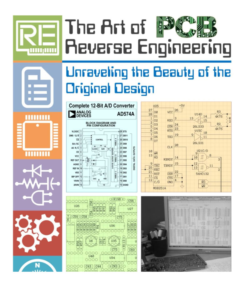

Professional Textbooks
Extensive textbooks and academic publications support
structured learning from theory to practice.

Specialized Equipment
Specialized reverse engineering tools and equipment
are actively developed and distributed worldwide.
Reverse Engineering
Applied Across All Industries
A core capability that supports localization, maintenance,
and technological self-reliance across industries.
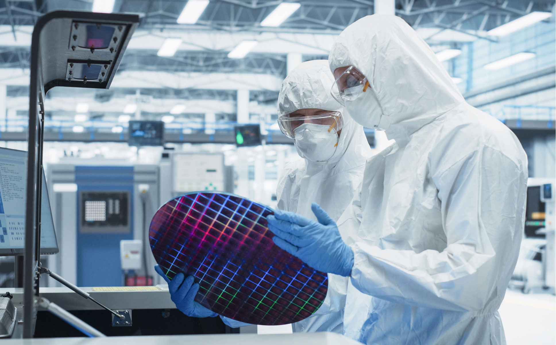
01
SEMICONDUCTOR MANUFACTURING
EQUIPMENT
Localization and enhancement of core PCB modules including RF
match, stage controller, MFC, and heater control boards.
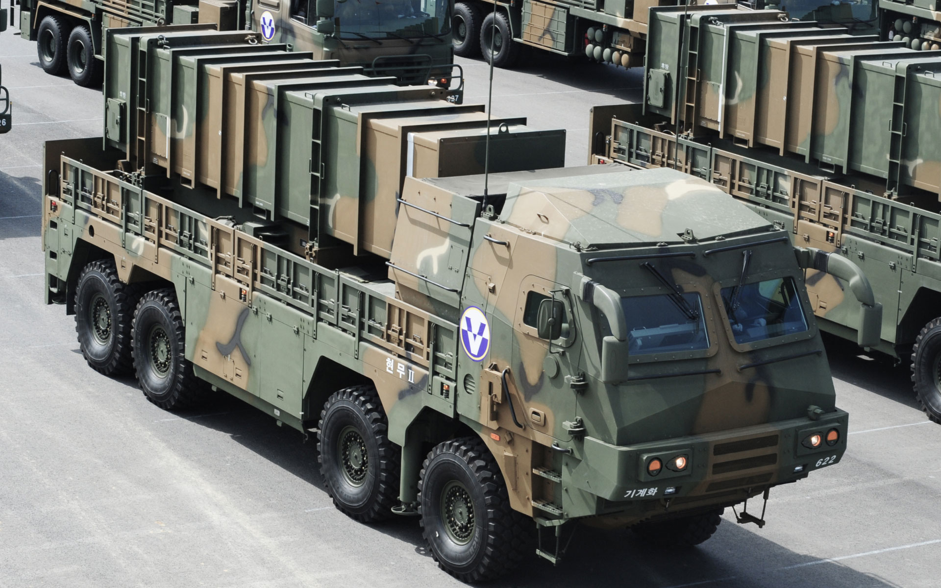
02
DEFENSE INDUSTRY
Analysis and redesign of defense electronic control modules based
on MIL-STD thermal, vibration, and EMI design technologies.

03
AUTOMOTIVE ELECTRONICS
Analysis and redesign of core automotive ECUs for localization and
performance improvement.
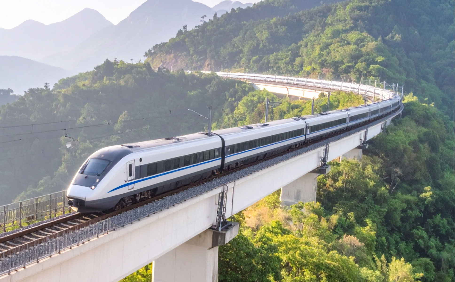
04
RAILWAY SYSTEMS
Localization and redevelopment of railway control units using
EN50121-based high-reliability design.

05
GENERAL INDUSTRY
High-precision PCB engineering solutions across plant, medical,
laser, robotics, and automation industries.
Technical Value

Shortest Development
Lead Time

Minimum Investment
Cost

High Technical
Accuracy

Acquisition of Advanced
Technology

Maximized Value &
Profitability
Creating new technological value
through innovation,
precision analysis,
and engineering insight.
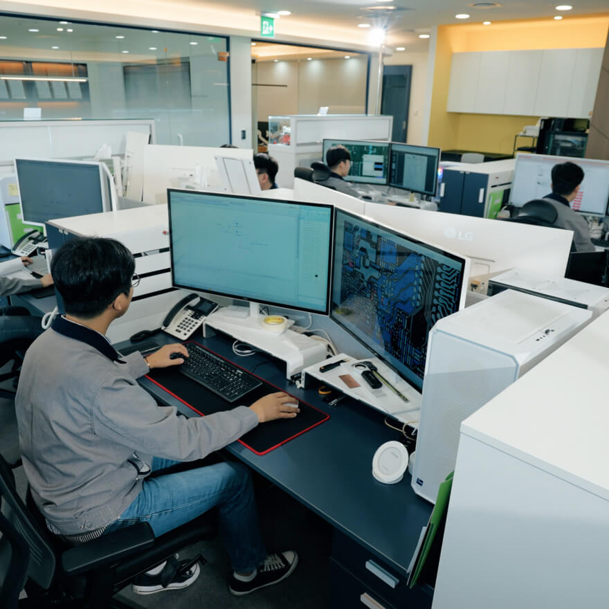
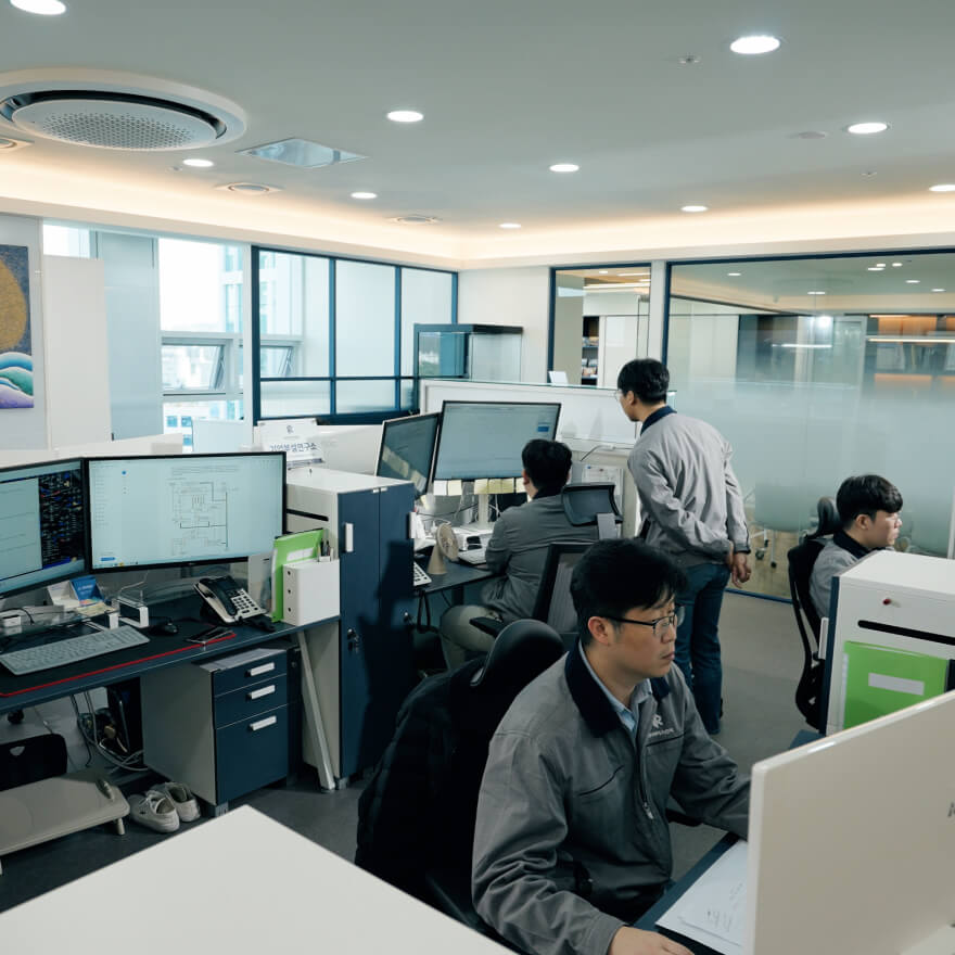
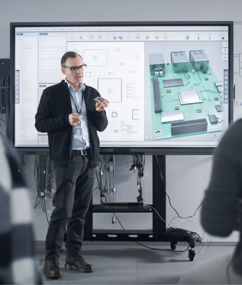
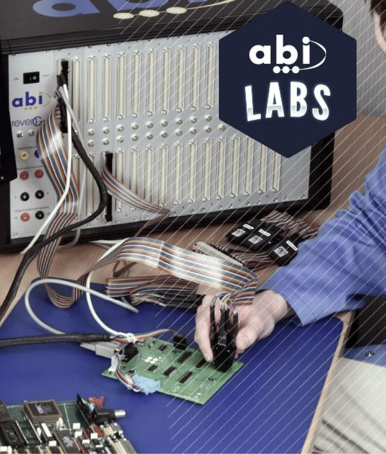
Process Workflow
End-to-end PCB reverse engineering
from design to prototype and verification.
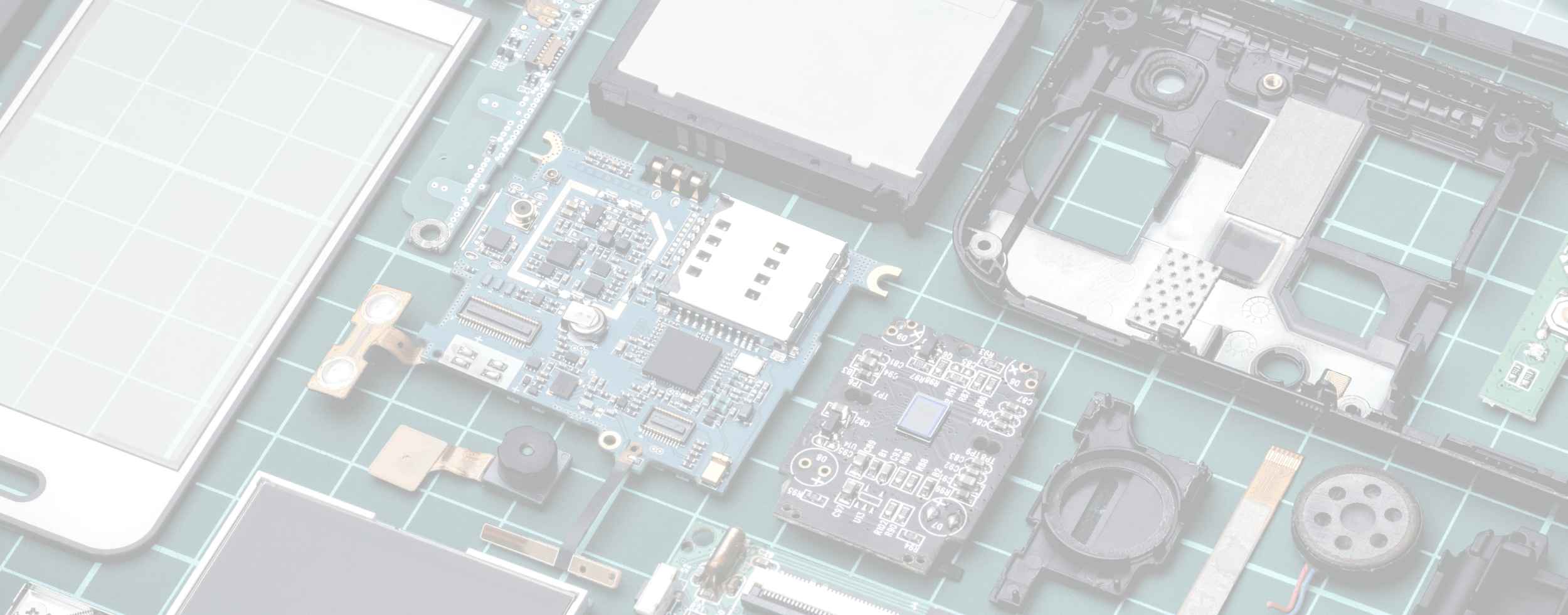
Sample Inspection
Check major components
and design architecture

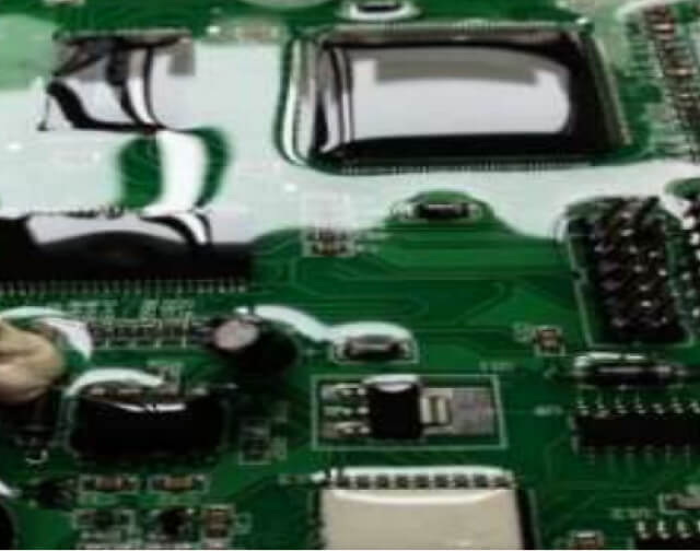
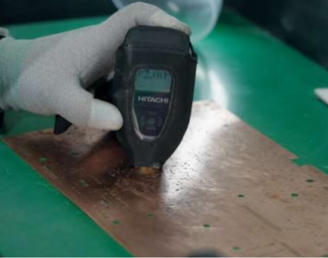
Coating Removal
Equipped with
technologies for removing
PCB insulation coating and
epoxy molding

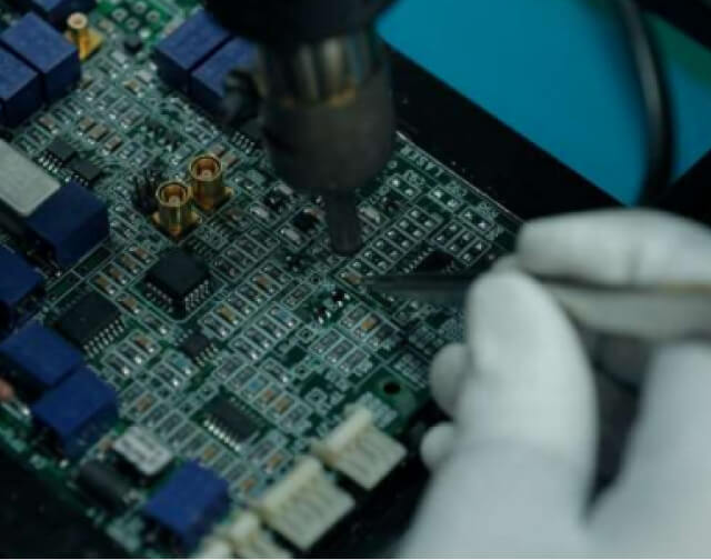
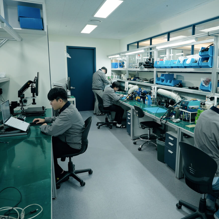
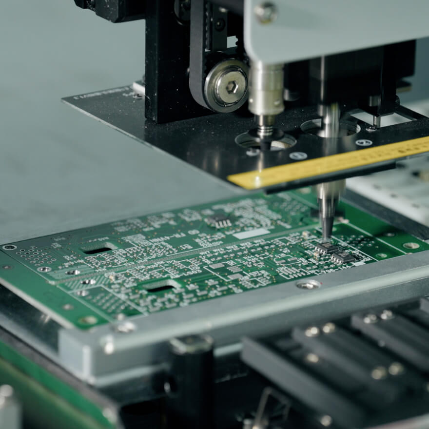
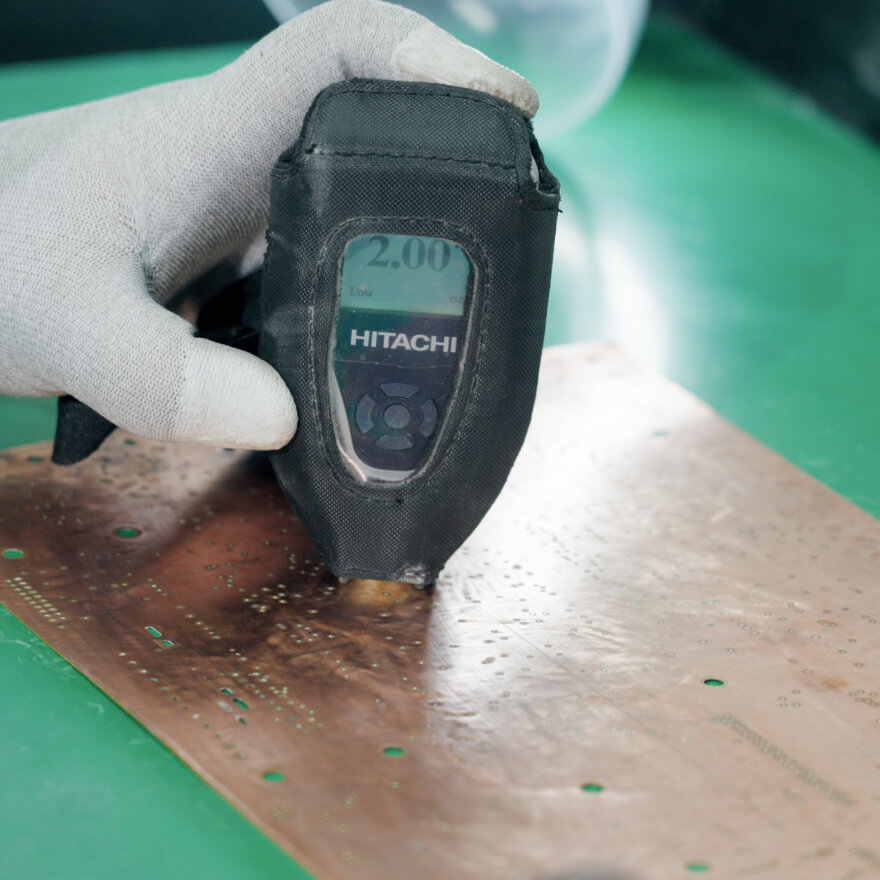
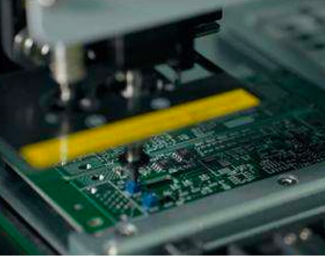
Component Removal
Performed by skilled
technicians, components
are removed safely and
stored without damage to
the original parts.

Firmware Extraction
We extract firmware from
fuse-protected MCUs
using ROM writers,
sockets, and dedicated
emulators.

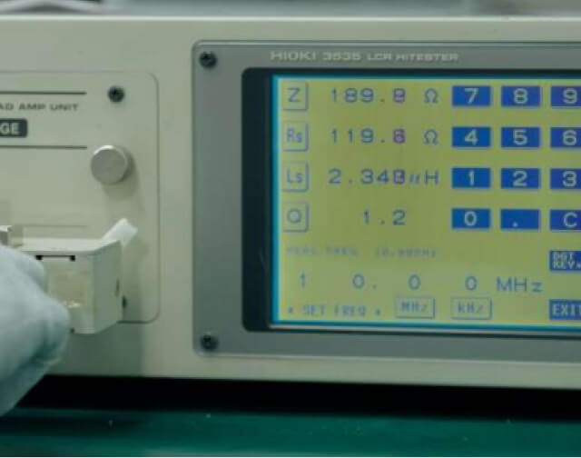
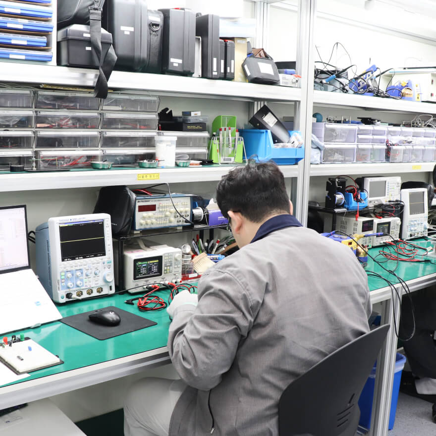
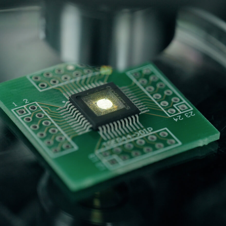
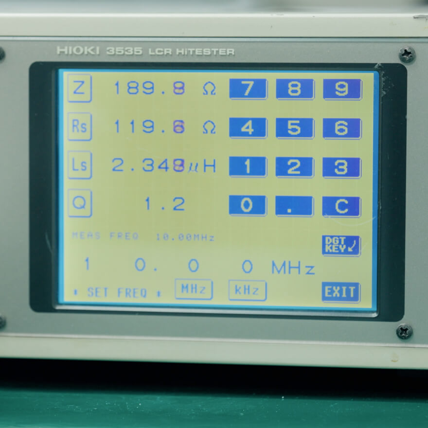
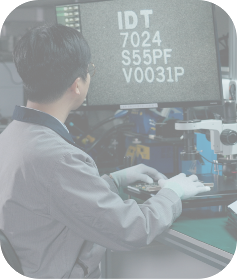
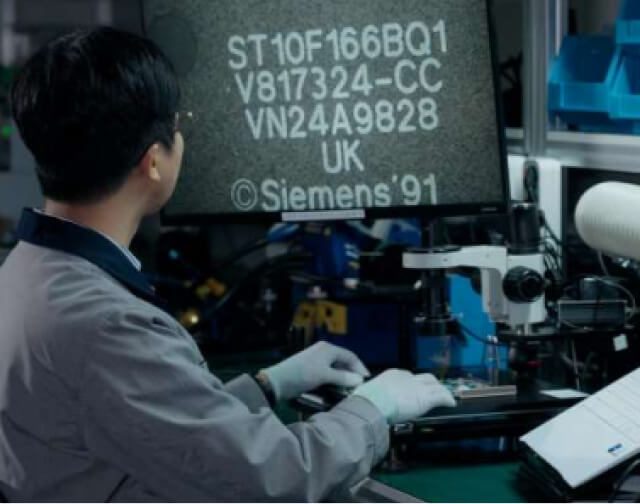
Component Analysis
Using an SMD marking code
database and professional
measuring equipment,
components are analyzed
quickly and accurately

Part List Documentation
Precise part names are
recorded, and
discontinued parts are
identified and replaced
with suitable alternatives.

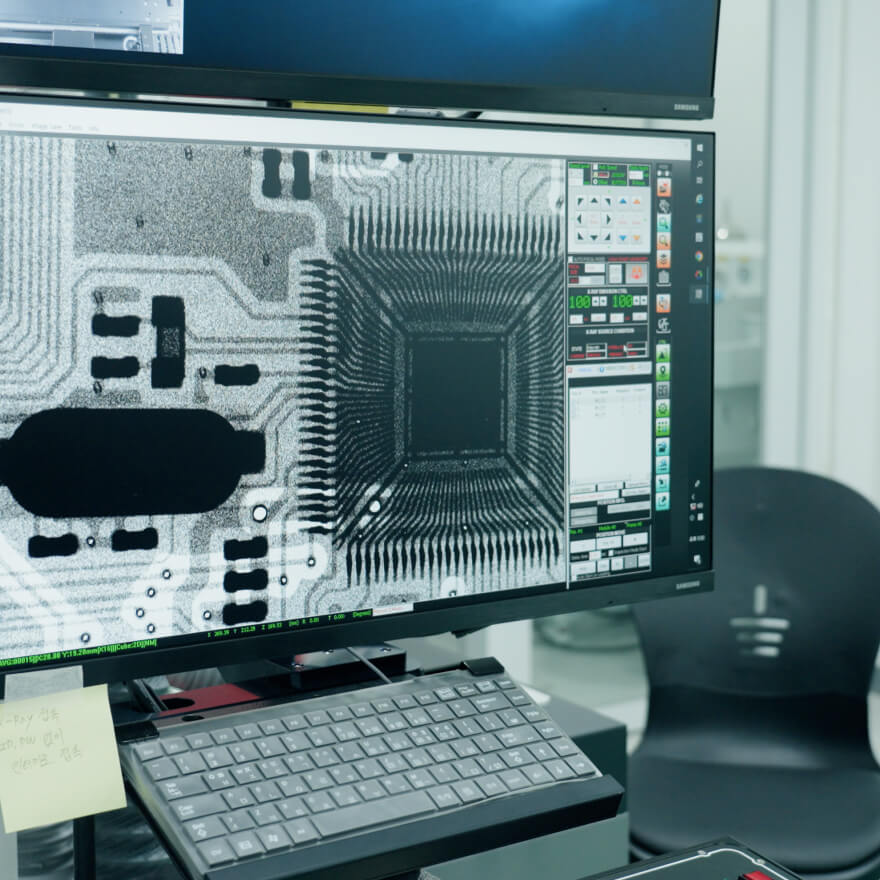
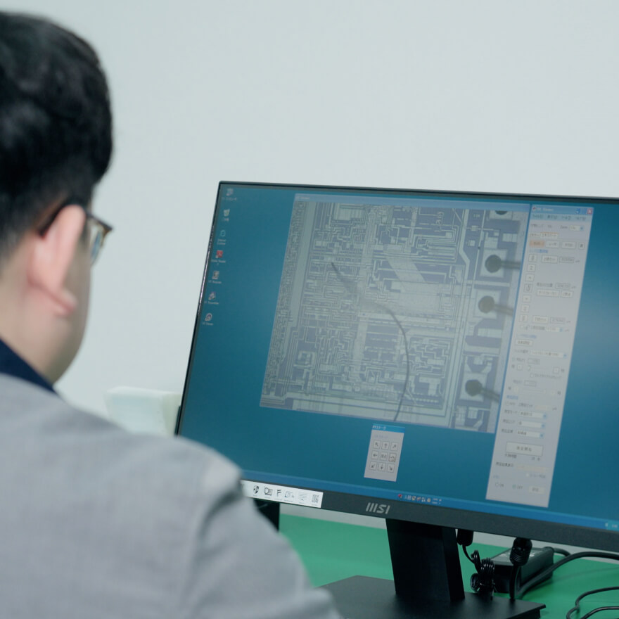
PCB Delayering
Layer patterns and
thickness are examined
for high-layer MLB and
build-up PCBs with 16+
layers.

ARTWORK
Scan images are converted
into 1:1 drawings, with
expertise in build-up PCBs,
high-speed impedance
boards, and ultra-multilayer
PCB artwork.

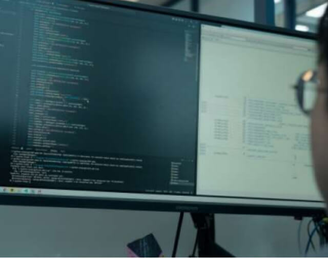
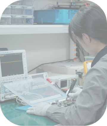
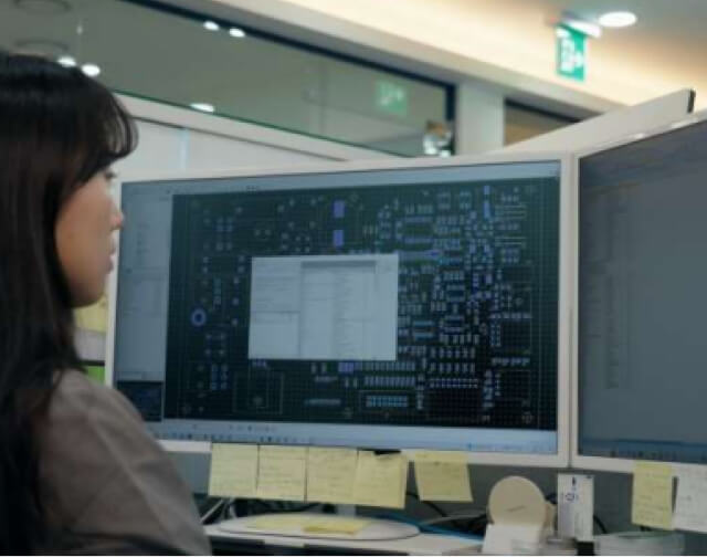
Schematic Extraction
High-quality circuit
drawings are created in
accordance with
schematic design rules,
delivering accurate and
reliable circuit diagrams

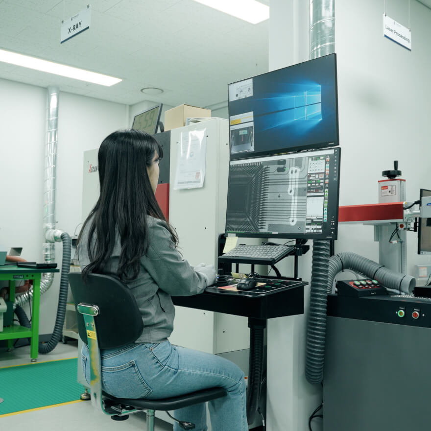
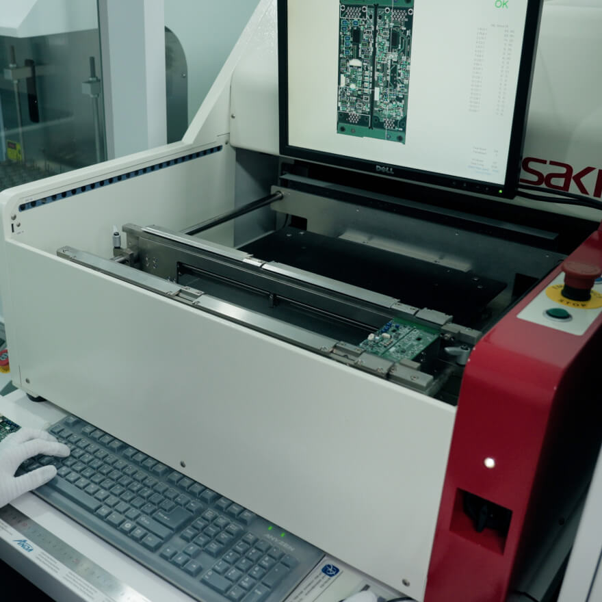
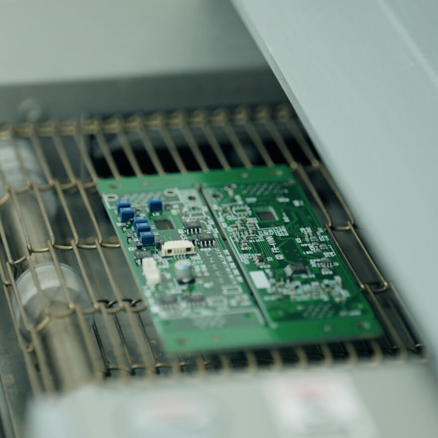
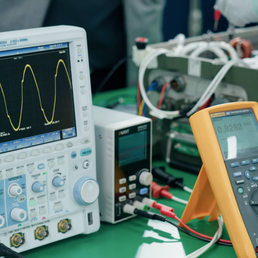
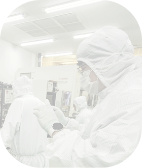
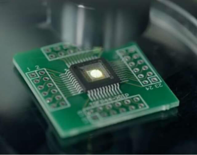
Prototype Manufacturing
Small-batch production
optimized with SMT, reflow,
inspection, and X-ray
systems for fast, high-quality
output.

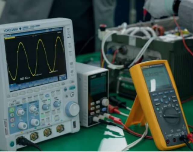
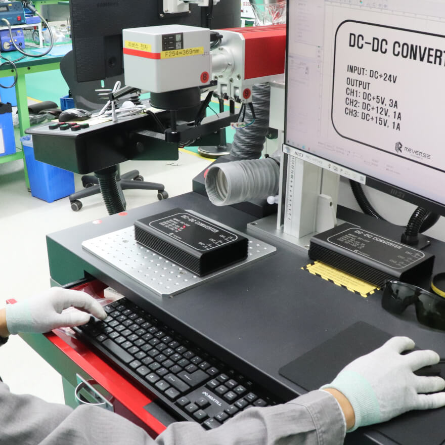
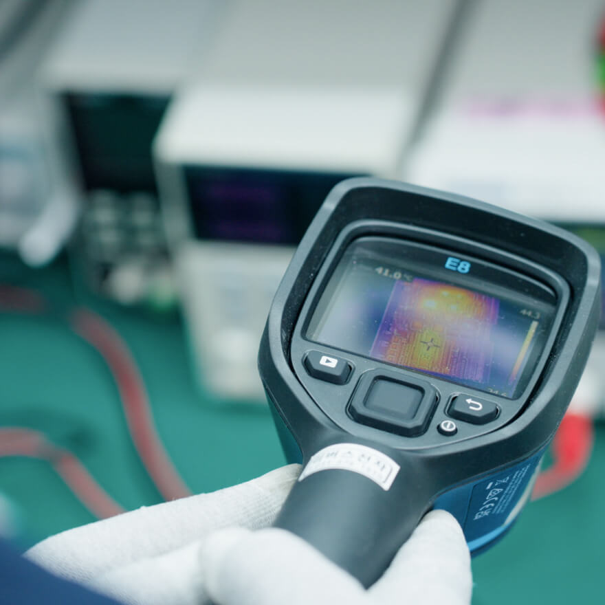
Performance Verification & Delivery
Performance is validated
to meet or exceed the
original product, followed
by field testing and final
delivery

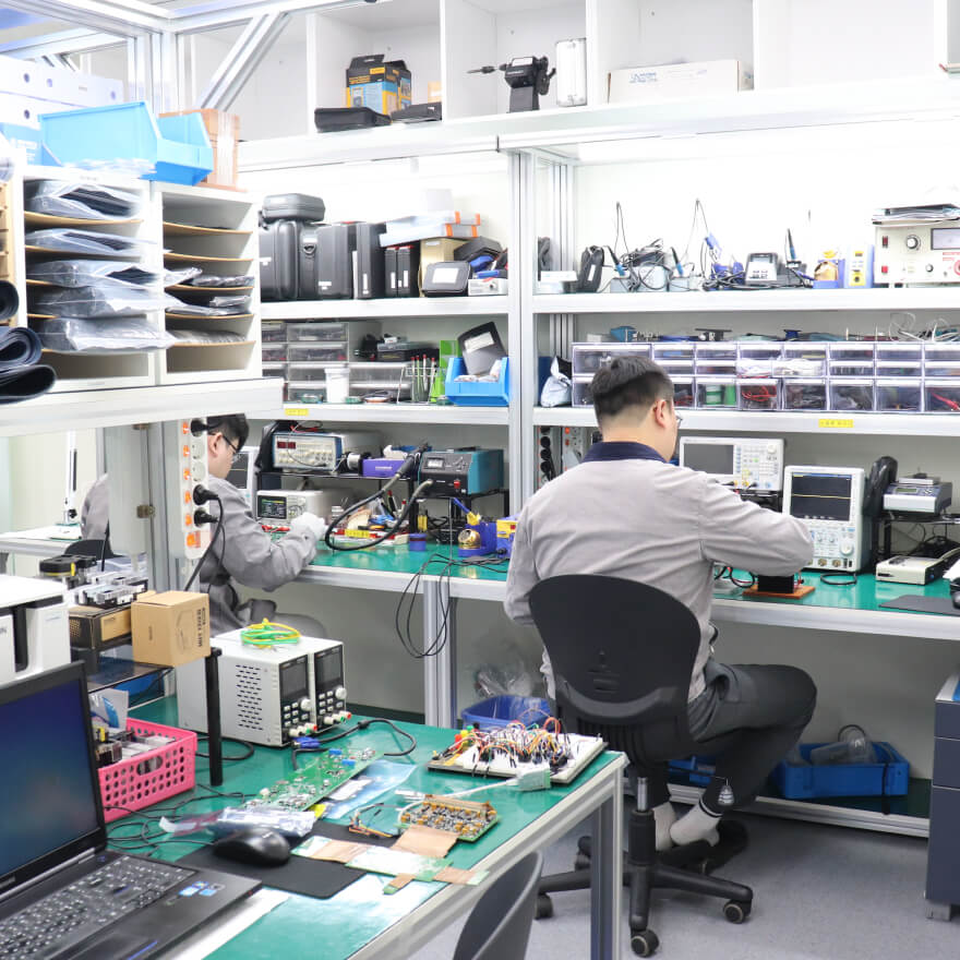
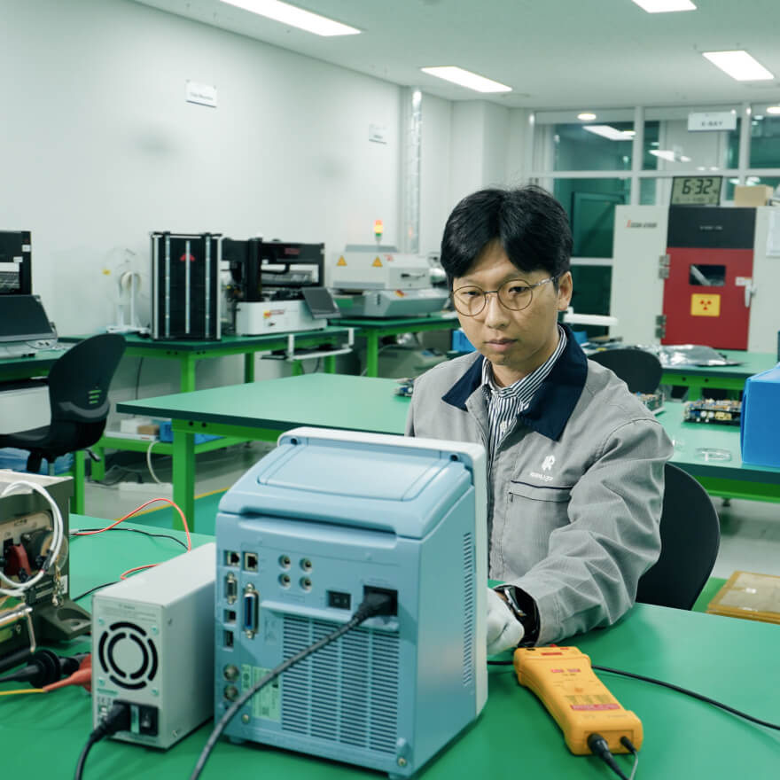
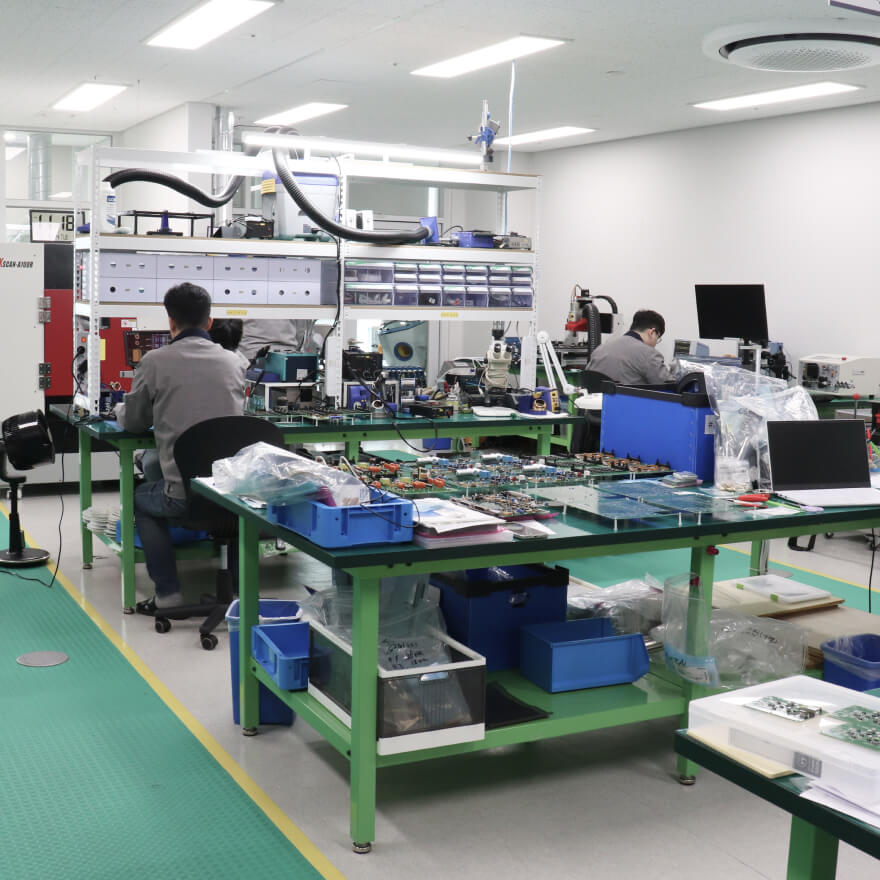
Facilities
Facilities optimized for small-batch production
with fast delivery and reliable quality.